New hardware crypto acceleration and protection functions extend the NXP LPC551x/S1x MCU’s security capabilities
By Saurin Choksi, Paul Kimelman and Durgesh PattamattaNXP Semiconductors
The latest on-demand webinar from NXP explains more about the security features of NXP’s LPC551x/S1x MCUs and the security requirements of edge IoT devices.
The demand for IoT security
With the advent of the IoT, connected devices are proliferating and billions of them are expected to go into service in the next few years. This trend of a connected world through IoT is bringing the need for security and asset protection to the smallest microcontrollers. Even simple edge-node IoT devices need security features, as shown in Figure 1, to support privacy, integrity, asset protection and access control.
In implementing security functions, cost and power are critical considerations for low- to mid-level MCUs in IoT edge devices. Processor cores based on the Arm® v8-M architecture with TrustZone® technology provide the fundamental building blocks with secure trusted execution. To build a secure system, however, additional features as described in Arm’s Platform Security Architecture (PSA) framework 6 are necessary.
NXP IoT security solutions
NXP offers products which use the Armv8-M-based Cortex®-M33 core and fulfil the PSA requirements. This article describes features of these LPC551x/S1x MCUs which contribute to the security capabilities of IoT edge nodes.

Fig. 1: the main security functions required in an IoT device
The CASPER crypto-accelerator
Signature generation and signature verification are mandatory steps for device certificate provisioning, secure boot and update. RSA2048 is a more commonly used algorithm for the signature function. Some applications, however, are moving to newer algorithms such as ECDSA for higher resistance to malicious attacks. Secure cloud connectivity makes ECC-based asymmetric key generation support a necessity: Elliptic Prime Curve 256b (EC_prime256v1), 384b (EC_secp384r1) and 521b (EC_secp521r1) are examples of the most in-demand curves.RSA- and ECC-based asymmetric cryptographic algorithms are compute-intensive (high operation count), inherently slow (for large and very large math operations) and power-hungry if executed purely in software.
Since asymmetric crypto-algorithms are primarily used in start-up routines or the session set-up phase, slow execution can extend a device’s boot time, wake-up time or pairing time. Pure hardware implementation is an alternative. These algorithms, however, continually evolve, and new curves are introduced on a regular basis to address the latest security threats; they involve more intense compute operations. This means that a fixed hardware solution can quickly become obsolete.
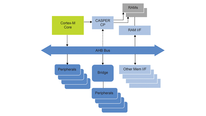
The CASPER crypto-accelerator solves this problem by providing an efficient hardware-software partitioning approach (see Figure 2). A generic engine, it can be applied to all types of cryptographic algorithms in combination with software, including:
- Asymmetric public-key (such as RSA and various flavours of ECC) and the related Diffie-Hellman key exchange methods
- Exponentials generating functions
- Non-standard large number algorithms
- In some cases, symmetric block ciphers, stream ciphers, and hashes
The CASPER cryptographic engine is normally used in conjunction with other standard hardware blocks for hashing (SHA) and symmetric cryptography (AES). It also offers flexibility to implement newer, non-supported crypto-algorithms, thereby providing performance and energy efficiency across various cryptographic uses.

Fig. 2: block diagram of the features of the CASPER security engine
The CASPER architecture has the following key features to optimise performance and energy efficiency.
1. Co-processor interface - the Cortex-M33 core provides a 64-bit wide co-processor interface. This interface allows the addition of an accelerator directly on the main CPU. This eliminates extra cycles of jobs to be submitted through the bus. CASPER can be accessed from the AHB bus, but also provides an interface to the Cortex-M33 core using the co-processor bus. Arm can kick-off CASPER using MCRR instructions and retrieve results using MRRC instructions.
This approach offloads the CPU from compute-intensive tasks, letting it sleep and allowing the system to run at a lower clock speed; or letting the CPU do other operations in parallel, such as setting up the next hardware operation while the previous one is being processed.
2. RAM access: CASPER can access system RAM using a dedicated 64-bit interface (2 x 32-bit interleaved RAMs in parallel) without going through the system bus. Since these RAMs are shared with system space, this interface can be used for other purposes when CASPER is not using it.
3. Multipliers and a bank of adders and registers: CASPER has Brent-Kung style adders for maximum efficiency (faster carry-out, lower power compared to CSLA) and 2 x 32-bit MUL-ADD type (extra rows for add) multipliers that are configured to allow for fast 64-bit x 64-bit multiplication in place, but using far fewer resources.
4. State machine: CASPER implements a state machine which performs operations such as multiply, modular multiply, reduce (Montgomery), add, sub, rsub, double, compare, compare-early-out, fill, zero, copy, re-mask-copy, modular add and subtract.
5. Masking for side-channel counter-measures: CASPER provides counter-measures against side-channel analysis by masking. Data is never stored in plain text when using masking with a random value. Masking is also used to flood adders and multipliers to obscure actual data processing.

Fig. 3: a system-level view of CASPER
CASPER’s hardware/software partitioning approach allows easier adaptation to new crypto-algorithms. By replacing the underlying math code of library Application Programming Interfaces (APIs) with direct hardware invocation, code porting is easy, and gives near-maximum performance gains.
The aim of CASPER is to optimize the execution of crypto-algorithms. Although simple use of a library is sufficient to use CASPER, code can be optimised to use the memory (64-bit RAM access) and to implement parallelisation to the full extent, and achieve the best performance and the lowest energy use.
To enable this, a special API library is developed to port Arm Mbed™ TLS functions to the CASPER acceleration features. CASPER functionality is made available to the user in three layers:
1. Casper_Driver: The base layer has init() and deinit() functions. It exports macros to generate co-processor instructions.
2. Casper_drive_pkha: This layer exposes Public/Private Key HW Acceleration (PKHA) routines. It accelerates a selected set of routines which could be used to optimise asymmetric cryptography operations. At present, NXP MCUs support the following:
- a. RSA signature verification
- b. ECC operations - ECDSA (sign, verify), ECDH and ECDHE for the following curves:
– Elliptic Prime Curve 256-bit (EC_prime256v1)
– Elliptic Prime Curve 384-bit (EC_secp384r1)
– Elliptic Prime Curve 521-bit (EC_secp521r1)
3. Mbed TLS library port: Port for the Mbed TLS library which uses casper_driver_pkha layer functions.
The user can develop additional support for crypto routines using API functions. Benchmarking between the NXP API for Mbed TLS running on CASPER versus pure software running on the CPU shows up to six times better performance for certain crypto operations (see Table 1).

Table 1: performance benchmarks for CASPER
On the same set-up, current measurements are shown in Table 2I. Thanks to performance improvements achieved through the use of CASPER, overall execution time is reduced and an energy reduction of up to 12 times is found in certain crypto operations.

Table 2: power benchmarks for CASPER
SRAM Physically Unclonable Function
Secret keys are fundamental to the security of MCUs. Traditionally, keys are stored in One-Time Programmable (OTP) eFuses, or in an alternative form of non-volatile storage. On the latest generation of NXP MCUs, however, a new type of key storage is provided using a Physically Unclonable Function (PUF). PUF provides secure key storage without storing the key.
Due to deep sub-micron process variations which are inherent in the production process, every transistor in SRAM cells has a random variation in electrical properties. This randomness is expressed in the start-up values of uninitialised SRAM memory, forming a unique chip fingerprint which is impossible to clone, but which is highly consistent at every power-up on a given die.
During operation, a small percentage of cells are inconsistent, creating randomness (<15%). With the use of error correction techniques such as helper data algorithms or fuzzy extractors, the PUF engine can generate a reliable root key from this unique but noisy digital fingerprint of the device derived from a dedicated SRAM.

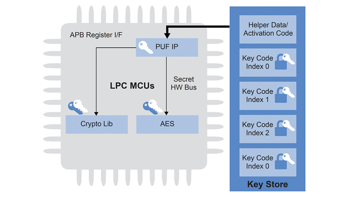
Fig. 4: SRAM PUF key storage
PUF comes with the following features:
- 1. Root key strength of 256-bits
- 2. Generation, storage, and reconstruction of random keys
- 3. Storage and reconstruction of user-provided keys
- 4. Key sizes from 64 to 4,096 bits
- 5. Key output via a dedicated secret key interface, or a register interface
The SRAM PUF algorithm has two modes: enrolment, and key reconstruction. Enrolment mode is typically executed once in the lifetime of the chip: the SRAM PUF response is read out and processed to generate the activation code (AC). The AC reveals no information about the key, and hence can be stored in any non-volatile memory.
The key reconstruction mode is used to retrieve the root key. This mode is also used to store any private information as a user key and retrieve it using the relevant key code (KC) as shown in Figure 4. The AC and KC are specific to an individual chip, and any change to codes prevents key reconstruction.
User keys can be used as the roots-of-trust for a set of other uses such as for protection of code IP, secure boot, secure update, or data protection. The PUF engine provides support for generating unique symmetric cryptographic keys for local usage (root key and session keys), or a seed for a DICE unique device secret key. The Key reference is unique for each die and key. The secret key output from the PUF is fed into symmetric cryptographic engines via a dedicated secret hardware bus. The PUF output is masked during transfer, offering a side-channel counter-measure.
Keys which are derived from the SRAM PUF are not stored on-chip but are derived from the chip only when they are needed. For this reason, they are only present in the chip for a very short period. When the SRAM is not powered, there is no key present on the chip. This makes the solution very secure.
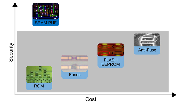
Figure 5 shows the SRAM PUF’s advantage compared to traditional methods for key storage. The SRAM PUF has proved to be resistant to various invasive and non-invasive physical attacks in security laboratories. Attacks with scanning electron microscopes, lasers, Focussed Ion Beams (FIBs) and probes have been unsuccessful. In addition, side-channel attacks have not led to any leakage of sensitive information.
A special anti-ageing technique assures that the behavior of the PUF is stable over the product’s lifetime.

Fig. 5: SRAM PUF compared to traditional key storage
The use of a PUF also simplifies device provisioning. With traditional OTP eFuse methods, these devices could not be used in any other product once provisioned, and must be scrapped if there was a problem with the provisioning process. With the introduction of the PUF, the secret key is already in the part and is only activated in the field without the risk of leaking the secret key. This helps make inventory management simpler and helps save cost by eliminating an additional key programming step during the manufacturing process.
PRINCE cryptographic algorithm
On-chip non-volatile storage contains many important assets. It is used to store secret keys, proprietary software from the silicon vendor and OEM, licensed application software and other sensitive information.
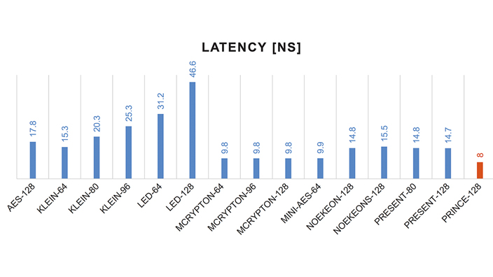
Traditionally, this storage is in plain-text format. This makes it easy for hackers to steal keys, read the code for cloning, or tamper with it to alter the execution sequence or programming value. This problem can be overcome by encrypting the Flash memory. Traditional encryption engines, such as AES, are slow however, require RAM, and would compromise system performance by adding latency.

Fig. 6: latency benchmark comparing PRINCE to other encryption engines

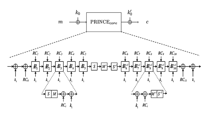
Fig. 7: PRINCE with 12-round block cipher PRINCE core
PRINCE is a lightweight symmetric block cryptography algorithm which can solve these problems. As shown in Figure 6, PRINCE is one of the lowest latency algorithms. The PRINCE is a 64-bit cypher with a 128-bit key. The concept behind the PRINCE encryption process is shown in Figure 7. The number of rounds can be configured to optimise the security/performance trade-off. RC is 64-bit round constants, K1 is the upper half of key, S is Sbox transform (S, S-1), M is matrix multiply (M, M`, M- 1).
NXP’s approach builds on the core PRINCE engine with 12 rounds, providing a robust implementation against various attacks. Since the algorithm became public in 2012, the PRINCE paper has received more than 500 citations, most of which are related to its security analysis. Neither theoretical nor practical attacks have been successful so far, which proves the security claims of the algorithm. The security level of PRINCE logarithmically decreases from 126 to 94 bits as a number of collected plain text-cipher text pairs increases from zero to 232 (32GB).
The PRINCE encryption key is updated before the 32GB of data have been encrypted, hence PRINCE-based memory encryption is seen to be practically as competitive as the industry-standard encryption algorithms.
Since the address is always available in advance compared to data, the address is used as an input vector to PRINCE together with a 128-bit key and 64-bit NONCE (Initialization vector, used only once for a given firmware version and region, unique to the device). This output cipher is XORed with the data for encrypted storage during a Write operation. The same is done for decryption during a read operation.
This CTR-based implementation provides a capability for zero-latency on-the-fly decryption, allowing the direct execution of instructions from an encrypted on-chip Flash region, and without the need for RAM buffers. Since PRINCE is used primarily for on-chip non-volatile storage of a firmware image, and the NONCE is changed with every image update, use of CTR does not create the vulnerability that is found in external non-volatile memory devices.
XEX mode would be used if encryption is for storage on an external memory. Additionally, code/data transfers from non-volatile memory to the CPU are masked when in cache, providing a counter-measure against side-channel attacks.
Sbox transform can be selected from many available variants and is updated from one product to another, providing additional obscurity and unique characteristics. In addition, 128-bit secret keys are fed to the PRINCE engine from the SRAM PUF via a hard-wired secret path. In combination with masking, they provide a counter-measure against side-channel attacks.

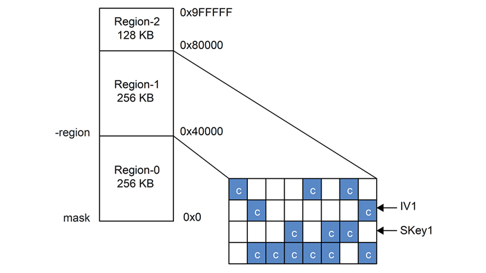
Fig. 8: the PRINCE secure memory regions
NXP’s implementation can support multiple unique encrypted memory regions with individual secret keys (see Figure 8). This isolation between regions allows system partners to separately store their proprietary software IP in non-volatile memory and guard against tampering or cloning. The start address for each encrypted storage region is programmable. Depending on the application, only certain parts of the region might need encrypted storage. To support this, further granularity with programmable control is defined within each region.
There is no observable difference between CoreMark® benchmarking performance on silicon with PRINCE on-the-fly decryption enabled compared to performance without PRINCE on-the-fly decryption (see Table 3). This proves that the PRINCE implementation offers zero-latency on-the-fly decryption, and does not incur any performance penalty. Also, power consumption is minimal.

Table 3: performance and power benchmarks for PRINCE
Summary
This paper introduced three unique features of the the latest generation of MCUs from NXP which help enable next-generation security with a minimal power and area penalty.
With CASPER and PUF combined, NXP’s latest generation of MCUs offer robust support for symmetric keys and asymmetric key-pair generation and management. PRINCE enables asset protection for an OEM’s proprietary software stored in non-volatile memory.
CASPER enables low-cost, high-efficiency hardware acceleration for ECC and RSA, and the hardware-software partitioning approach offers sufficient flexibility to accommodate new algorithms on existing devices.
SRAM-PUF provides a way to authenticate devices and generate and store cryptographic keys from an unclonable silicon fingerprint. It offers a scalable solution which also simplifies provisioning.
PRINCE is a lightweight cipher which enables encryption of Flash memory and on-the-fly, zero-latency decryption, with minimal area and power cost and without compromising system performance.


