New Fabrication Process for Ultra-Low Power MCUs Set to Boost Usage of Energy-Harvesting Technologies
The Renesas RE01 development board provides a ready-to-use platform for designers to experiment with energy harvesting in new projects
With the Renesas RE01 development board, there is a new silicon process technology for fabricating silicon devices which draw very low currents both in active and in stand-by mode, while providing high processor performance with low-voltage operation. This new Silicon On Thin Buried Oxide (SOTB) process enables the development of a new generation of ultra-low power semiconductor devices, including a new family of Renesas microcontrollers which can operate completely from a harvested energy source.
The SOTB process is a distant relative of the Fully Depleted - Silicon On Isolator ( FD-SOI ) technology, which is typically used to manufacture Systems-on-Chip (SoCs) and Application Specific Standard Products (ASSPs). Devices which are fabricated in an FD-SOI process tend to offer high levels of integration and high clock rates. While operating current can be impressively low, they are not normally considered to be low-power devices. Generally they also do not allow for the integration of non-volatile on-chip memory technologies such as Flash.
The SOTB process overcomes these drawbacks, supporting the design of a new generation of battery-powered MCUs aimed at applications that require both high levels of processing performance, integrated memory and low active and stand-by power consumption. These MCUs are ideal for any intelligent, connected application such as IoT sensors.
Most MCUs today are fabricated in a CMOS bulk silicon process. These processes have a long history and their strengths and weaknesses are well understood. Figure 1 shows a comparison between SOTB and the standard bulk silicon processes used to implement MCUs today, at a variety of process geometries.

Fig. 1: process technologies and their active and leakage current values
MCU manufacturers can choose to use an advanced process node, typically with a line width of 40nm or less, to gain the advantage of high levels of peripheral integration, with large on-chip Flash memory of 2Mbytes or more, along with high clock rates of >200MHz.
While the active switching current of such a process is very low, at around 50-100µA/MHz, the leakage current from each gate in such a small process node is very high, resulting in high stand-by current of typically 10-100µA, or sometimes even higher.
For many applications, especially those that use a battery, or applications using harvested energy, low stand-by current is often the most important parameter. If this is the key requirement for the design, the MCU would normally be produced in a process with a larger line width: this restricts both performance and integration of memory and other peripherals. Clock rates of <80MHz are typical, and memory sizes normally restricted to <512kbytes. These processes may have drawing active current of 250-500µA/MHz, while the leakage current can be in the range of a few hundred nanoamps.
The new Renesas SOTB process marks a breakthrough in low-power technology: MCUs fabricated on the process can offer active-mode current of <20µA/MHz, and leakage current of as little as 120nA, while still allowing the development of devices with high clock rates and large embedded Flash memory and SRAM provision.
This combination of integration and power consumption will make devices developed on this process ideal for battery-powered applications but also for applications that use energy-harvesting power sources. It will probably reduce overall energy usage by as much as a factor of ten compared to a device fabricated in a standard CMOS bulk silicon process.
New Hybrid Silicon Structure
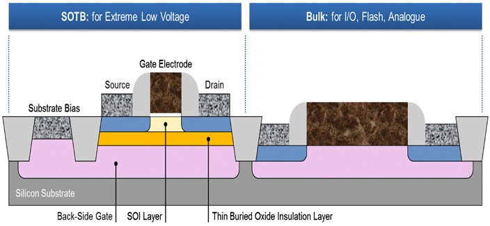
One of the huge breakthroughs in the development of this technology has been the creation of a hybrid silicon structure: this combines the benefits of the new SOTB process and the existing standard bulk silicon technology in the same design (see Figure 2). This allows Renesas to exploit the strengths of both technologies on the same device, and to provide ultra-low power MCUs which include on-chip Flash memory.
The use of the hybrid structure means that Renesas can use the new ultra-low power SOTB technology for the gates in the kernel area, implementing such key logic components as the CPU and peripherals, enabling them to consume the lowest possible power.
Standard bulk silicon gates can still be used for features such as the I/O ring and analogue components, for which a high drive voltage might be required.
This means that designers can easily work with these new devices, as they will have similar electrical characteristics to today’s MCUs.

Fig. 2: Renesas’ hybrid structure comprised of SOTB and bulk silicon segments
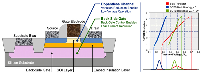
Figure 2 shows some of the benefits of the SOTB gate structure. In a traditional CMOS bulk silicon gate design, channel impurities or dopant atoms are injected into the silicon during the manufacturing process. The dopant enables the gate to conduct when required. The number of atoms injected into each gate is hard to control accurately, and this means that the gate threshold characteristics can vary greatly across a device.
This is a problem particularly at small silicon geometries, when the number of atoms involved is extremely small, sometimes as few as 100 atoms. There can be substantial variation in the number of dopant atoms in each gate, resulting in varying switching characteristics across the device’s millions of gates.
The SOTB process eliminates this problem by using a dopantless channel design. The characteristics of the gate are controlled by the thin oxide layer within the gate. In a modern fabrication process, this layer is well controlled and thus repeatable across the device.
This means that the variation between each gate is much lower than with the traditional bulk silicon gate design. As will be seen below, this reduction in the variation between gates on a SOTB device allows Renesas to greatly reduce the operating voltage and hence the energy used to switch the gate. This limit in variation between the gates on the device also has several other important benefits, such as a reduction in the noise generated between pairs of gates within the device. This noise reduction also enhances the performance of the analogue elements of the device.
The thin SOI layer also has some additional benefits, as it provides extra protection from errors caused by cosmic rays. The software error rate on these devices is markedly better than that of similar devices at the same process node.
Figure 3 shows another benefit of the SOTB technology: the ability to apply a negative back bias voltage to each gate. This allows us to manipulate the switching thresholds of each gate on the device, either individually or across the total device.

Fig. 3: comparison of the threshold voltage in the SOTB process and the standard bulk silicon process
The graph on the left-hand side of Figure 3 shows the threshold voltages for both a standard CMOS bulk gate and an SOTB gate. The red line shows the range of switching characteristics for a typical device implemented on a bulk silicon process; here we show the variation in switching threshold between 1 million transistors on the test device. The diagram reveals that the best gates will switch at around 0.3V, while the worst gates will switch at around 0.7V. The difference is due to the inherent variability of the process.
This means that, to guarantee the operation of every gate on the device, we must operate at a voltage markedly higher than 1.0V. This of course has a direct impact on the power consumed by the device.
The blue line in Figure 4 shows the characteristics of the SOTB gate. It reveals how the process greatly reduces switching variability and ensures switching characteristics are maintained within a narrow range. A device based on the SOTB process can run safely at a much lower voltage while guaranteeing that every gate will operate correctly, resulting in a huge drop in active power consumption.
The green line in Figure 4 shows the result of the back bias being applied: this enables gates to be put individually into a very low leakage state, greatly reducing stand-by current.
Thanks to the SOTB process, Renesas can develop a new generation of MCUs which combine the best qualities of smaller-geometry devices, which offer a high level of integration and low active current, and larger-geometry devices, which have low leakage current. Renesas has now finished development of the RE01, the first MCU to use the SOTB process. It offers a unique combination of performance, integration and power consumption.
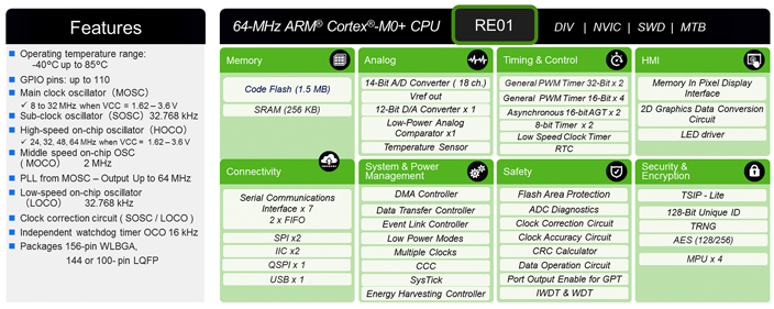
The first RE01 device combines an Arm® Cortex®-M0+ core running at up to 64MHz with a high level of peripheral integration. It features up to 1.5Mbytes of Flash and 256kbytes of on-chip SRAM. Renesas has a roadmap for the introduction of additional devices featuring smaller memory provision for sensors, and devices with an on-chip Bluetooth® Low Energy radio.
The use of the SOTB technology on this new device has resulted in some remarkable low-power characteristics:
- Active current of between 20µA and 35µA/MHz
- Stand-by current of 120nA
- ADC operation at 4µA at 32kHz
- 256kbyte SRAM with less than 1nA/kbyte stand-by current

Fig. 4: the Renesas RE01 MCU fabricated in the SOTB process
The new Renesas RE01 with its unique combination of large on-chip Flash memory and on-chip SRAM, along with ultra-low power consumption levels and small package sizes including the 4.1mm x 4.3mm WLBGA package (see Figure 5), will make the RE01 ideal for a wide range of applications, such as:
- Smart and hybrid watches
- Wearable devices
- IoT sensors
- Medical sensors
- Industrial sensors
- Building and home automation
- Structural monitoring sensors
It is in fact ideal for use in any product for which ultra-low power and small package size are important.

RE01 MCU’s WLBGA package
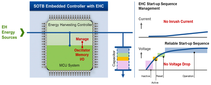
The first SOTB-based embedded controller will enable powerful, connected devices to source energy from the environment, and each member of the RE01 family will have an Energy Harvesting Controller (EHC) on-chip. This unique peripheral allows the microcontroller to start from an energy-harvesting source, and to manage external rechargeable batteries or supercapacitors to provide a power reservoir.
Many problems have to be resolved when designing an energy-harvesting application: one of the biggest problems when using a normal MCU is managing the start-up current. Normally an energy source can only supply a small amount of current at any time, and typically a normal MCU will take substantially more current than is available from the energy source during the start-up phase.
The EHC on the RE01 can manage this start-up current and the whole start-up sequence, so the MCU starts up reliably and safely (see Figure 5).

Fig. 5: the operation of the RE01 MCU’s Energy Harvesting Controller
The RE01 can run fully on an energy-harvesting power source. The device can operate with a wide range of potential energy sources including solar power, vibration, pressure, and temperature difference. The EHC, supported by very few external components, completely manages the cyclic wake-up sequence of the MCU with the very low harvested source current.
The EHC includes internal inrush current protection, and can operate at a very low voltage to avoid malfunctions during the start-up phase.
Designers can easily start to develop low-power applications with the RE01 using the new RE01 evaluation board available from Future Electronics, which has the part number RTK70E015DS00000BE. The evaluation board includes an RE01 CPU with all its I/Os available on connectors. The board supports an Arduino Uno interface as well as two Pmod interfaces: both are ideal for adding hardware functions. A Pmod MiPs display interface is also included in the kit. The board also includes an on-board J-Link debugger to allow users to easily debug their applications.
For developers who want to experiment with energy harvesting, the evaluation board comes with an additional interface designed to enable various harvested power sources to be connected: the board is supplied with a small solar cell which can be used to power the board. The board also has interfaces to allow external supercapacitors or rechargeable batteries to be added to enable the user to develop a complete energy-harvesting system.
Conclusion
The use of SOTB oxide technology enables Renesas to provide devices with unique characteristics which make them ideal for energy-harvesting applications. The combination of low power consumption, both in active and stand-by mode, along with the large on-chip memory and high-performance CPU, will allow users to develop powerful solutions for the next generation of applications, and will provide solutions for applications we cannot yet imagine.
Readers may apply for an RTK70E015DS00000BE development kit for the RE01 family of MCUs via Future Electronics’ my-boardclub.com website.


