
 Orders shipping outside of United States will be on hold while the company evaluates tariff impacts.
Please contact your salesperson for assistance.

Faster, better, cheaper. For years, this has been the goal of suppliers and manufacturers in the electronics industry, resulting in rapid gains in productivity across a variety of markets and applications. Camera manufacturers are no exception to this rule, as the ability to quickly and efficiently bring new camera models to market can provide a clear competitive advantage.
One of the easiest ways to do this is through the use of a platform camera design, in which the architecture of a single camera system is used as the basis for multiple end products. For many years, ON Semiconductor has worked to enable this type of family approach to industrial cameras. For example, many of ON Semiconductor’s Interline Transfer Charge-Coupled Device (CCD) image sensors share a common architecture which allows a single camera design to use different image sensors. Likewise, cameras based on the PYTHON family of CMOS image sensors can be configured with any one of eight different values for resolution, from VGA to 25Mpixels, with just two different PCB design variants.
But what if this design flexibility could be extended to include other product parameters as well as resolution? This is the goal of ON Semiconductor’s new X-Class CMOS image sensors, which enable a single camera design to support different pixel features as well as different resolution values, as shown in Figure 1. Now, a single camera design can be scaled not only for the number of pixels in the image sensor but also the type of pixel used. Characteristics of the pixel functions that the designer can specify include:
- Global shutter/rolling shutter
- Enhanced dynamic range
![]()
Fig. 1: The X-Class image sensors provide a choice of pixel features as well as a choice of resolution
As long as the pixel is in the common high-speed, low-power frame used across the X-Class platform, a single camera design can support it, speeding time-to-market for new camera designs and simplifying supply-chain logistics.
The first pixel to be deployed in this platform is a new 3.2μm design which combines excellent global-shutter imaging performance with low noise and high dynamic range. This X-Class Global Shutter (XGS) pixel enables the development of high-resolution, high-performance industrial image sensors in a compact size.
For instance, the new XGS 8000 and XGS 12000 image sensors offer the small package size and low-power operation needed for use in 29mm x 29mm camera designs. The differences between the two devices are in resolution and frame rate:
- The XGS 12000 is in a 1" optical format providing resolution of 12Mpixels at up to 90 frames/s
- The XGS 8000 is in a 1/1.1" optical format, and provides full 4K/UHD resolution (4096 x 2160 pixels) at up to 130 frames/s
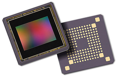
Fig. 2: The XGS family image sensors are offered in small land grid array packages
Since both are available not only in monochrome and color configurations but also in different speed grades, the most appropriate configuration can be matched to a given application, whether for general machine vision purposes such as inspection and industrial automation, or for broadcast or surveillance.
So the X-Class platform gives camera manufacturers a new design flexibility, changing how camera designs can be configured to support multiple products. As additional XGS resolutions and pixel options are added to the X-Class platform in the future, camera manufacturers will be able to quickly build from a single camera design to support additional product resolutions and features in a cost-effective manner.
In other words: faster, better, and cheaper.
 |
 |
