
![]() Free shipping within the continental US over $50. Conditions apply
Free shipping within the continental US over $50. Conditions apply
 Orders shipping outside of United States will be on hold while the company evaluates tariff impacts.Please contact your salesperson for assistance.


Manufacturer Part #
MC74VHCT125ADR2G
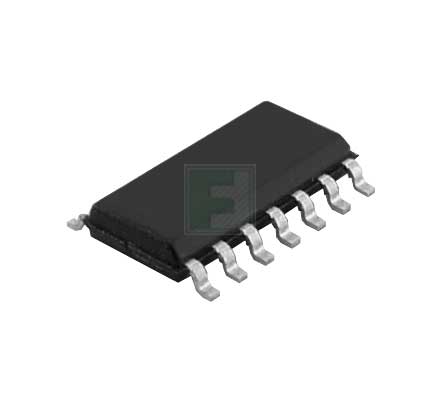
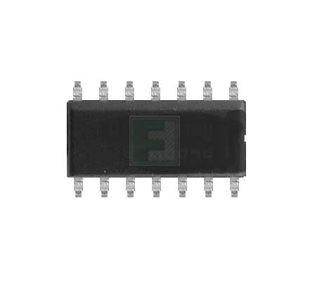
74VHC Series 5.5 V Quad Bus Buffer with 3−State Control Inputs - SOIC-14
|
|
|||||||||||
|
|
|||||||||||
| Mfr. Name: | onsemi | ||||||||||
| Standard Pkg: |
Product Variant Information section
Available PackagingPackage Qty:2500 per Reel Package Style:SOIC-14 Mounting Method:Surface Mount |
||||||||||
| Date Code: | |||||||||||

onsemi MC74VHCT125ADR2G - Product Specification
Shipping Information:
HTS Code:
ECCN:
PCN Information:
Part Status:
-
https://futureelec.wufoo.com/forms/?formname=r8bzou01ws8brs&field12=NA&field16=en&field2=MC74VHCT125ADR2G&field4=onsemi&field18=https://p1na.futureelectronics.com/p/logic--74-series--a-vhc-t/mc74vhct125adr2g-on-semiconductor-6508758

-
https://futureelec.wufoo.com/forms/?formname=r8bzou01ws8brs&field12=NA&field16=en&field2=MC74VHCT125ADR2G&field4=onsemi&field18=https://p1na.futureelectronics.com/p/logic--74-series--a-vhc-t/mc74vhct125adr2g-on-semiconductor-6508758

onsemi MC74VHCT125ADR2G - Technical Attributes
| Logic Circuit: | Buffer |
| Family: | A/VHC/T/U |
| No of Functions / Channels: | 4 |
| Output Characteristics: | 3-ST |
| Supply Voltage-Nom: | 4.5V to 5.5V |
| Package Style: | SOIC-14 |
| Mounting Method: | Surface Mount |
Features & Applications
The MC74VHCT125A is a high speed CMOS quad bus buffer fabricated with silicon gate CMOS technology. It achieves high speed operation similar to equivalent Bipolar Schottky TTL while maintaining CMOS low power dissipation. The MC74VHCT125A requires the 3-state control input (OEbar) to be set High to place the output into the high impedance state.
The VHCT inputs are compatible with TTL levels. This device can be used as a level converter for interfacing 3.3V to 5.0V, because it has full 5V CMOS level output swings.
The VHCT125A input structures provide protection when voltage between 0V and 5.5V are applied, regardless of the supply voltage. The output structures also provide protection when VCC = 0V. These input and output structures help prevent device destruction caused by supply voltage - input/output voltage mismatch, battery backup, hot insertion, etc.
The internal circuit is composed of three stages, including a buffer output which provides high noise immunity and stable output. The inputs tolerate voltages up to 7V, allowing the interface of 5V systems to 3V systems.
Features:
- High Speed: tPD = 3.8 ns (Typ) at VCC = 5.0 V
- Low Power Dissipation: ICC = 4.0 µA (Max) at TA = 25°C
- TTL-Compatible Inputs: VIL = 0.8 V; VIH = 2.0 V
- Power Down Protection Provided on Inputs
- Balanced Propagation Delays
- Designed for 2.0 V to 5.5 V Operating Range
- Low Noise: VOLP = 0.8 V (Max)
- Pin and Function Compatible with Other Standard Logic Families
- Latchup Performance Exceeds 300 mA
- ESD Performance:Human Body Model > 2000 V;Machine Model > 200 V
- Chip Complexity: 72 FETs or 18 Equivalent Gates
- Pb-Free Packages are Available
Available Packaging
Package Qty:
2500 per Reel
Package Style:
SOIC-14
Mounting Method:
Surface Mount