R5F563NDDDFP#V0 in Tray by Renesas | 32 bit | Future Electronics
text.skipToContent text.skipToNavigation

Manufacturer Part #

R5F563NDDDFP#V0

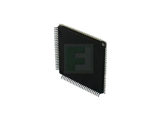
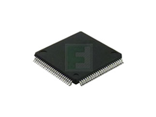
RX63N Series 1.5 MB Flash 128 kB RAM 100 MHz 32-Bit Microcontroller - LQFP-100

ECAD Model:
Mfr. Name: Renesas
Standard Pkg:
Product Variant Information section
Date Code:
Product Specification Section
Renesas R5F563NDDDFP#V0 - Technical Attributes
Attributes Table
Family Name: RX63N
Core Processor: RX
Program Memory Type: Flash
Flash Size (Bytes): 1.5MB
RAM Size: 128kB
Speed: 100MHz
No of I/O Lines: 79
InterfaceType / Connectivity: CAN/Ethernet/I2C/SCI/SPI/USB
Peripherals: CAN/Ethernet/I2C/On-Chip-ADC/On-Chip-DAC/SCI/SPI/USB/Watchdog
Number Of Timers: 26
Supply Voltage: 2.7V to 3.6V
Operating Temperature: -40°C to +85°C
On-Chip ADC: 8-chx10-bit / 14-chx12-bit
On-Chip DAC: 2-chx10-bit
Watchdog Timers: 1
Package Style:  LQFP-100
Mounting Method: Surface Mount
Features & Applications

The R5F563NDDDFP#V0 is a single-precision 32 bit floating-point processing unit with 128 KB RAM, 1536KB program memory, It incorporates communication functions suitable for networking equipment.

It can operates on a dedicated power supply as a low power feature, standby power consumption can be reduced by 90% compared to existing products. The selection of on-chip memory has been expanded from ROMless to 2 MB and available in smaller-sized  LQFP-176 packages.

Features:

  • 32-bit RX CPU core
    • Max. operating frequency: 100 MHz
    • Capable of 165 DMIPS in operation at 100 MHz
    • Single precision 32-bit IEEE-754 floating point
    • Low-power design and architecture
    • Operation from a single 2.7- to 3.6-V supply
    • Low power consumption 500 μA/MHz
  • On-chip main flash memory, no wait states
    • Supports ROM-less versions and versions with up to 2 Mbytes of ROM
    • 100-MHz operation, 10-ns read cycle (no wait states)
    • 384-Kbyte to 2-Mbyte capacities
    • User code programmable via the USB, SCI, or JTAG
  • On-chip data flash memory
    • ROM-less or 32 Kbytes of ROM
    • Programming/erasing as background operations (BGOs)
  • On-chip SRAM, no wait states
    • 32- to 128-Kbyte capacities
  • DMA
    • DMAC: Four channels
    • DTC
    • EXDMAC: Two channels
    • External address space
    • Buses for high-speed data transfer (max. operating frequency of 50 MHz)
    • 8 CS areas (8 × 16 Mbytes)
    • Multiplexed address data or separate address lines are selectable per area.
    • 8-, 16-, or 32-bit bus space is selectable per area
    • Independent SDRAM area (128 Mbytes)
  • Up to 20 extended-function timers
    • 16-bit MTU2: input capture, output compare, PWM waveform output,phase-counting mode (6 channels)
    • 16-bit TPU: input capture, output compare, phase-counting mode (12 channels)
    • 8-bit TMR (4 channels)
    • 16-bit compare-match timers (4 channels)
  • A/D converter for 1-MHz Operation
    • Up to 21 12-bit channels, and incorporating 1 sample-and-hold circuit
    • Up to 8 10-bit channels, and incorporating 1 sample-and-hold circuit
    • Addition of results of A/D conversion (in the 12-bit converter)
    • Self diagnosis (for the 10-bit converter)
  • 10-bit D/A converter: 2 channels
  • Temperature sensor for measuring temperature within the chip
  • Register write protection can protect values in important registers against overwriting.
  • Up to 134 pins for GPIO
  • 5-V tolerance, open drain, input pull-up, switchable driving ability
  • Operating temp. range
  • –40°C to +85°C

Applications:

  • Ethernet controller
  • USB 2.0 full-speed (function, host, or OTG selectable)
  • CAN
Read More...
Pricing Section
Global Stock:
0
USA:
0
On Order:
0
Factory Stock:Factory Stock:
0
Factory Lead Time:
12 Weeks
Minimum Order:
180
Multiple Of:
90
Total
$2,282.40
USD
Quantity
Unit Price
180+
$12.68
Product Variant Information section