
 Orders shipping outside of United States will be on hold while the company evaluates tariff impacts.
Please contact your salesperson for assistance.


By: Mike Becker, International Product and Marketing Manager, Power MOSFETs, Nexperia
Low cost power supplies are used in abundance to power a wide range of consumer and industrial applications such as mobile phones, tablet computers, notebook computers, rechargeable power tools and LED lighting, to name just a few.
The efficiency of a power supply is often the most important major design factor, whether high efficiency is needed to meet legislative requirements, or also maybe to reduce the dissipated heat in order to facilitate a reduced form factor, e.g. size and weight. Choosing a synchronous MOSFET to meet all of the requirements can be a bewildering task.
When selecting a MOSFET for a switching application, engineers often look at the obvious datasheet parameters first, e.g. what size and type of package is needed, what voltage is needed (don’t ignore the spike!), and what is the maximum output current (determines the I2R losses at the rated load current, and hence the MOSFET’s RDS(on) also).
Maybe a few of the dynamic parameters will be considered also; for example, gate charge (Qg and Qgd) can be a good indicator of the expected gate losses. The Qg-FOM (figure of merit) is also a good indicator of a MOSFET’s efficiency in a switching application, and the MOSFET’s capacitance (Ciss, Coss, Crss) can help to indicate whether drain-source spiking and gate bounce will be an issue. Low capacitance can contribute to higher efficiency also.
There is another parameter, Qrr, which can generally be found lurking at the bottom of the datasheet and is often ignored. In applications where current flows through the MOSFET’s body diode, for example, in a synchronous rectifier and in free-wheel applications, then the reverse recovery charge (Qrr) causes some significant issues as discussed below, which the design engineer needs to carefully address.
What is Qrr?
QRR is stored charge (measured in nC), and is caused by charge carriers accumulating in the body diode’s PN junction when the diode is forward biased.


Beware of Qrr!
Due to the dead-time needed in most applications, current flows through the body diode twice for every switching cycle.
In the first instance, we can consider what happens just before the sync-fet is turned on. Since current will be flowing through the body diode during the dead-time, then some of the load current becomes trapped as stored charge (Qrr).
As the sync-fet is turned on, then the stored charge is dissipated internally within the MOSFET. Therefore, a proportion of the load current is lost due to the Qrr effect and becomes an I2R loss within the sync-fet.

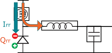
In the second instance, the MOSFET’s body diode becomes reverse biased once again when the high-side MOSFET turns on. Additional current (Irr + load current) flows briefly through the high-side MOSFET until the stored charge (Qrr) is fully depleted. The charge depletion is not instantaneous, and the reverse recovery time (Trr) is also quoted on the datasheet.
Irr typically flows for a few tens of nS until Qrr is depleted. Irr results in additional I2R losses within the high-side MOSFET as per the following diagram:
VDS Spiking
Reverse recovery current (Irr) also interacts with the PCB’s parasitic inductance to create a voltage spike where V = L x (di/dt).

The MOSFET should be suitably rated to ensure that the BVDS rating is higher than the maximum spike; typically an 80% derating is applied. An application with a measured 80V V-DS spike would typically require a MOSFET with BVDS of at least 100V.
Good PCB layout can reduce the parasitic inductance (L), and choosing a low Qrr MOSFET can help to reduce the di/dt also. If spiking is ignored, then this may result in a higher voltage grade MOSFET being required.
Gate Bounce
When VDS spiking occurs, then designers should also look for ‘gate bounce’ in their application. Since there is capacitance between all 3 terminals of a MOSFET, then any spiking at the drain pin will also be capacitively coupled to the MOSFET’s gate pin. In extreme cases, if the ‘gate bounce’ exceeds the MOSFET’s threshold voltage VGS(th) then the MOSFET can turn on.
Dead-time is usually applied in the gate drive circuits to ensure that the high-side and low-side MOSFET cannot be turned on at the same time. However, when gate-bounce occurs, then the low-side MOSFET is turned on at the same time as the high-side, causing ‘shoot-through’ current to flow between the power supply rails, resulting in excessive I2R losses and in extreme cases causing destruction of the MOSFET.
Benefits of Low Qrr MOSFETs
MOSFETs are not all the same! A quick comparison of MOSFET vendors’ datasheet parameters for 100V MOSFETs with 4~8mΩ RDS(on) shows that there are dramatic differences in Qrr between different vendors.
Other vendors are typically 130% to 300% higher Qrr than similar RDS(on) types with NextPower 100V technology.
Since it is difficult to measure the individual Qrr effects in a typical application, then we rely on simulations to model the effects instead.
Spice simulations for a 7mR MOSFET (PSMN6R9-100YSF) show that when Qrr is increased by 2x, the resultant spike voltage can increase by around 8%.

Choosing a MOSFET with low Qrr can also significantly improve the efficiency. Especially at low load current (<5 Amps), choosing a low Qrr MOSFET gives significant efficiency gains, since the dynamic losses are more significant than I2R losses in this portion of the efficiency curve.

Conclusion
In low-power chargers and adapters, where load currents are typically less than 5A, then there is less emphasis on I2R losses, and design engineers should pay more attention to the dynamic losses also.
In conclusion, choosing a MOSFET with low Qrr can result in lower spiking, improved efficiency and reduced EMI emissions.
NextPower 100V MOSFETs offer very low Qrr as well as competitive RDS(on), and are ideally suited to power supply applications.
Choose from:
| LFPAK56 | TO220 | I2PAK |
|---|---|---|
| PSMN5R6-100YSF | PSMN8R5-100PSF | PSMN8R5-100ESF |
| PSMN6R9-100YSF | PSMN018-100YSF | PSMN018-100ESF |
| PSMN8R7-100YSF |
 |
| RECENTLY ADDED TO YOUTUBE |
 |